PS4 Controller PCB Circuit Board diagram includes JDM-001, JDS-001, JDM-011, JDS-011, JDM-020, JDM-030, JDS-030, JDM-040, JDS-040, JDM-050, JDS- 050, JDM-055, JDS-055, Circuit Board and USB/LED board
The JDM-001 (1-889-300-11 (Blue PCB) or 1-889-300-21 (Green PCB))


The JDS-001 board, aka USB/LED board.


Vias for the buttons of the JDM-001 (NOTE: The PCB is the Blue version here, but the Blue and the Green boards are identical in this respect)
NOTES on button layout, applies to all versions so far..
The D-pad, Cross, Circle, Square and Triangle buttons are active Lo. Connecting them to any Ground spot will make them work.
The L1 and R1 are Active Hi, and have to be connected to the 3.2v line to activate.
The L2 and R2 are PWM and should connect to the 2L and 2R spots respectively if they are to be duplicated.

Then the JDM-011 (1-893-557-21 or 1-893-557-31) is the second one I’ve seen. It’s a little smaller width wise and has some things moved around, but is pretty much the same thing. The USB/LED board (not pictured yet) is redone so there are 2 less wires on the connector. The shell has also been changed for the smaller PCB, so a 1:1 swap can’t be done without some modification to this version shell if installing one of the older wider boards.


The JDS-011 board, aka USB/LED board.


Vias for the buttons of the JDM-011

The JDM-020 (1-893-899-11) is the latest revision. They seem to have ditched the Fujitsu ARM for a Freescale one and finally started to use blind vias.


NOTE: Because the JDM-020 uses blind vias, I’ll need to have one of these to tear down and see about the best spots for duplicate buttons and such.
Well, here are the X, O, /\ and [ ] Vias.


New DS4 version board (mid/late July 2015) This thing has had a pretty decent change made to the shell and the Daughter board layout. The Daughter board has been split into a 2 piece design now and connects on the sides of the mother board versus the middle as every previous version has. The core way of how the controller works hasn’t changed though.
JDM-030 (1-980-146-11)


The JDS-030 board, aka USB/LED board.


Here are the X, O, /\ and [ ] Vias.

Latest DS4 version board for the Slim console (mid September 2016) Again with a change made to the shell and the Daughter board layout. The Daughter board has gone back to a single piece design (not interchangeable with older versions) and it connects around the top left of the board versus the middle.
When my other board arrives, I’ll remove the ARM to see if there is a via for Square button. The Cross, Circle and Triangle buttons have them for sure, but you’ll only get 1 shot at them, and if you’re not up for that small work, I designed the SFX-040, so no soldering is required on the controller PCB at all.
JDM-040 (1-981-330-31)


The JDS-040 board, aka USB/LED board.


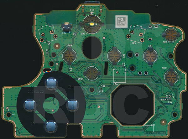
JDM-050 (1-982-355-11 and 1-982-355-21)


The JDS-050 board, aka USB/LED board.

DM-055 (1-982-707-11, 1-982-707-22, 1-982-707-31, 1-982-707-32, 1-982-707-81)
1-982-707-31 Schematic


The JDS-055 board, aka USB/LED board.

Vias locations for the X, O, /\ and [ ] buttons. JDM-050 shown here, but the JDM-055 spots are in the identical locations, even though the board is slightly different. Any ground spot can be used for the common connection.
NOTE: Be aware though, if the via is ruined in the process, repairing the controller will be extremely difficult if not impossible. The SFX-040 that was made for the JDM-040 version (above) will also work on the -050 and -055 versions here if you’re not wanting to risk it.